- 您现在的位置:买卖IC网 > Sheet目录1917 > DSPIC30F3013-20I/ML (Microchip Technology)IC DSPIC MCU/DSP 24K 44QFN
PIC18F46J11 FAMILY
DS39932D-page 144
2011 Microchip Technology Inc.
TABLE 10-8:
SUMMARY OF REGISTERS ASSOCIATED WITH PORTC
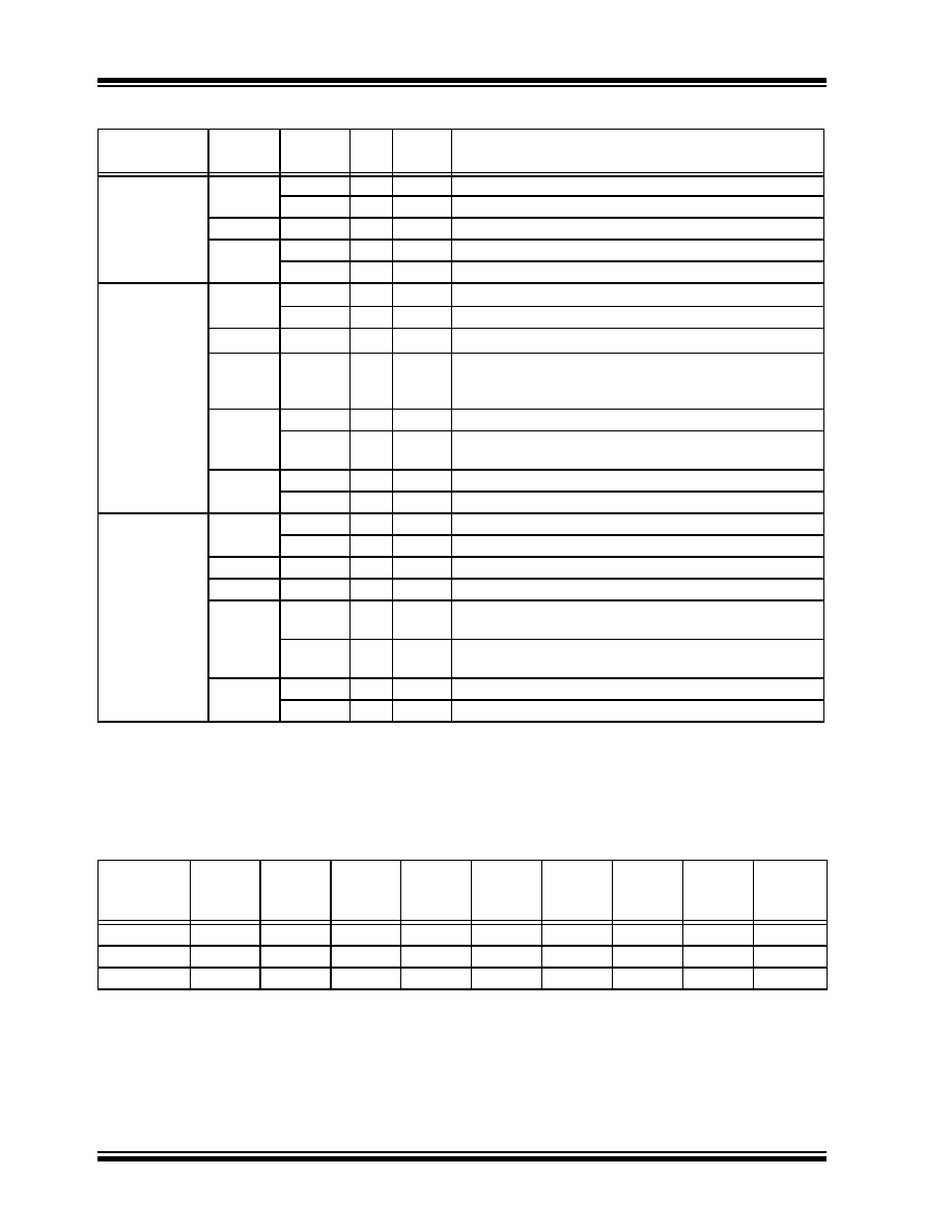
RC5/SDO1/
RP16
RC5
1
I
ST
PORTC<5> data input.
0
O
DIG
LATC<5> data output.
SDO1
0
O
DIG
SPI data output (MSSP1 module).
RP16
1
I
ST
Remappable peripheral pin 16 input.
0
O
DIG
Remappable peripheral pin 16 output.
RC6/PMA5/
TX1/CK1/RP17
RC6
1
I
ST
PORTC<6> data input.
0
O
DIG
LATC<6> data output.
PMA5(1)
0
O
DIG
Parallel Master Port address.
TX1
0
O
DIG
Asynchronous serial transmit data output (EUSART
module); takes priority over port data. User must configure
as output.
CK1
1
I
ST
Synchronous serial clock input (EUSART module).
0
O
DIG
Synchronous serial clock output (EUSART module); takes
priority over port data.
RP17
1
I
ST
Remappable peripheral pin 17 input.
0
O
DIG
Remappable peripheral pin 17 output.
RC7/PMA4/
RX1/DT1/RP18
RC7
1
I
ST
PORTC<7> data input.
0
O
DIG
LATC<7> data output.
PMA4(1)
0
O
DIG
Parallel Master Port address.
RX1
1
I
ST
Asynchronous serial receive data input (EUSART module).
DT1
1
ST
Synchronous serial data input (EUSART module). User
must configure as an input.
0
O
DIG
Synchronous serial data output (EUSART module); takes
priority over port data.
RP18
1
I
ST
Remappable peripheral pin 18 input.
0
O
DIG
Remappable peripheral pin 18 output.
TABLE 10-7:
PORTC I/O SUMMARY (CONTINUED)
Pin
Function
TRIS
Setting
I/O
Type
Description
Legend:
DIG = Digital level output; TTL = TTL input buffer; ST = Schmitt Trigger input buffer; ANA = Analog level
input/output; I2C/SMB = I2C/SMBus input buffer; x = Don’t care (TRIS bit does not affect port direction or
is overridden for this option)
Note 1:
This bit is only available on 44-pin devices.
Name
Bit 7
Bit 6
Bit 5
Bit 4
Bit 3
Bit 2
Bit 1
Bit 0
Reset
Values
on page:
PORTC
RC7
RC6
RC5
RC4
RC3
RC2
RC1
RC0
LATC
LATC7
LATC6
LATC5
LATC4
LATC3
LATC2
LATC1
LATC0
TRISC
TRISC7
TRISC6
TRISC5
TRISC4
TRISC3
TRISC2
TRISC1
TRISC0
发布紧急采购,3分钟左右您将得到回复。
相关PDF资料
DSPIC30F4011-30I/ML
IC DSPIC MCU/DSP 48K 44QFN
DSPIC30F4013-30I/ML
IC DSPIC MCU/DSP 48K 44QFN
DSPIC30F5013-30I/PT
IC DSPIC MCU/DSP 66K 80TQFP
DSPIC30F5015-30I/PT
IC DSPIC MCU/DSP 66K 64TQFP
DSPIC30F6010-20E/PF
IC DSPIC MCU/DSP 144K 80TQFP
DSPIC30F6010A-30I/PF
IC DSPIC MCU/DSP 144K 80TQFP
DSPIC30F6013A-30I/PF
IC DSPIC MCU/DSP 132K 80TQFP
DSPIC30F6014-30I/PF
IC DSPIC MCU/DSP 144K 80TQFP
相关代理商/技术参数
dsPIC30F3013-20I/SO
功能描述:数字信号处理器和控制器 - DSP, DSC 28LD 20MIPS 24 KB RoHS:否 制造商:Microchip Technology 核心:dsPIC 数据总线宽度:16 bit 程序存储器大小:16 KB 数据 RAM 大小:2 KB 最大时钟频率:40 MHz 可编程输入/输出端数量:35 定时器数量:3 设备每秒兆指令数:50 MIPs 工作电源电压:3.3 V 最大工作温度:+ 85 C 封装 / 箱体:TQFP-44 安装风格:SMD/SMT
dsPIC30F3013-20I/SP
功能描述:数字信号处理器和控制器 - DSP, DSC 28LD 20MIPS 24 KB RoHS:否 制造商:Microchip Technology 核心:dsPIC 数据总线宽度:16 bit 程序存储器大小:16 KB 数据 RAM 大小:2 KB 最大时钟频率:40 MHz 可编程输入/输出端数量:35 定时器数量:3 设备每秒兆指令数:50 MIPs 工作电源电压:3.3 V 最大工作温度:+ 85 C 封装 / 箱体:TQFP-44 安装风格:SMD/SMT
DSPIC30F3013-30I/ML
功能描述:数字信号处理器和控制器 - DSP, DSC Sensor RoHS:否 制造商:Microchip Technology 核心:dsPIC 数据总线宽度:16 bit 程序存储器大小:16 KB 数据 RAM 大小:2 KB 最大时钟频率:40 MHz 可编程输入/输出端数量:35 定时器数量:3 设备每秒兆指令数:50 MIPs 工作电源电压:3.3 V 最大工作温度:+ 85 C 封装 / 箱体:TQFP-44 安装风格:SMD/SMT
DSPIC30F3013-30I/SO
功能描述:数字信号处理器和控制器 - DSP, DSC Sensor RoHS:否 制造商:Microchip Technology 核心:dsPIC 数据总线宽度:16 bit 程序存储器大小:16 KB 数据 RAM 大小:2 KB 最大时钟频率:40 MHz 可编程输入/输出端数量:35 定时器数量:3 设备每秒兆指令数:50 MIPs 工作电源电压:3.3 V 最大工作温度:+ 85 C 封装 / 箱体:TQFP-44 安装风格:SMD/SMT
DSPIC30F3013-30I/SO
制造商:Microchip Technology Inc 功能描述:IC DSC 16BIT 24KB 40MHZ 5.5V SOIC-28
DSPIC30F3013-30I/SP
功能描述:数字信号处理器和控制器 - DSP, DSC Sensor RoHS:否 制造商:Microchip Technology 核心:dsPIC 数据总线宽度:16 bit 程序存储器大小:16 KB 数据 RAM 大小:2 KB 最大时钟频率:40 MHz 可编程输入/输出端数量:35 定时器数量:3 设备每秒兆指令数:50 MIPs 工作电源电压:3.3 V 最大工作温度:+ 85 C 封装 / 箱体:TQFP-44 安装风格:SMD/SMT
DSPIC30F3013-30I/SP
制造商:Microchip Technology Inc 功能描述:16-Bit Digital Signal Controller
dsPIC30F3013T-20E/ML
功能描述:数字信号处理器和控制器 - DSP, DSC 44LD 20MIPS 24 KB RoHS:否 制造商:Microchip Technology 核心:dsPIC 数据总线宽度:16 bit 程序存储器大小:16 KB 数据 RAM 大小:2 KB 最大时钟频率:40 MHz 可编程输入/输出端数量:35 定时器数量:3 设备每秒兆指令数:50 MIPs 工作电源电压:3.3 V 最大工作温度:+ 85 C 封装 / 箱体:TQFP-44 安装风格:SMD/SMT